MUSIC Lab at SUSTech
Home | People-Openings | Teaching | Research-Publications | Outreach | Facilities | Resources
News
» [10 Apr 2019] » Dr. Xiaomeng Gao receives the Best Young Professional Paper Award at WAMICON2019
» [01 Feb 2019] » DART Lab to Advance to Phase 3 of the DARPA SPAR Program
» [23 May 2018] » Songjie Defended his PhD Degree
» [20 Jan 2018] » DART Lab to Advance to Phase 2 of the DARPA SPAR Program
» [07 Mar 2017] » DART Lab Awarded NSF STTR Phase II Project on Developing a Radar-based Wearable Heart Health Monitoring Device
» [08 Nov 2016] » DART Lab to Participate in DARPA SPAR program
Integrated Circuits
Tunable N-Path Integrated Filters with Enhanced Blocker Rejection
Although passive filters, such as surface acoustic wave (SAW) filters, film bulk acoustic resonator filters, and the evanescent-mode tunable filters mentioned above, offer excellent filtering performances in terms of rejection, passband flatness, and linearity, their relatively large physical size prevents them from being integrated with the active circuits. In recent years, N-path filters have regained interest because of its potential in providing very high filter shape factors within integrated circuit processes. The most unique characteristics for N-path filters is that their center frequency is determined by the clock frequency, therefore allowing for extremely wide tuning range often approaching 10:1.
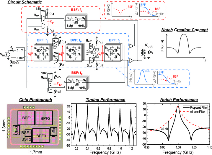
Using an N-path resonator as a building block, we have been investigating advanced tunable on-chip RF filter designs. In several recent works, we have proposed and demonstrated the capability of creating very notch frequencies very close to the filter passband. This is achieved by the parallel combination of one N-path bandpass filter and one N-path bandstop filter. The interferometric cancellation of the signals traveling through the two paths results in sharp rejection bands. In the actual design implemented in a 65-nm CMOS process, the parasitic capacitances lead to less attenuation in the notch bands, which can be compensated by introducing tuning elements (switches) in the baseband capacitors and by adding an additional signal cancellation path.
Passive Devices and Circuits
Highly Reliable Hot-Switching RF-MEMS Direct-Contact Switches
Due to its low insertion loss, high isolation, high linearity, wide bandwidth, and near-zero dc power consumption, radio frequency micro-electromechanical (RF-MEMS) switches have been an emerging technology with significant potential in many high frequency circuits and systems, especially those requiring reconfiguration. Compared to other high frequency switching technologies, metal contact RF-MEMS switches have the highest figure of merit (FoM, defined as 1/RonCoff) because of its ultimately low contact resistance and off-state capacitance. In addition, metal contact RF-MEMS switches have extremely large bandwidth that can extend from dc to beyond 100 GHz.
However, the reliability issues associated with RF-MEMS contact switches have been a major barrier for the wider adoption of the technology. Significant efforts have been devoted to improving the lifetime (primarily in terms of cycling time) of RF-MEMS contact switches. For example, the Radant MEMS switch can be cycled up to 100 billion times under cold-switching conditions. Under hot-switching conditions, however, the reliability of these switches degrades quickly with a sharp increase in contact resistance and insertion loss after a few tens of thousands of cycles. For applications where hot switching is needed, improving the reliability of RF-MEMS switches has been a significant challenge.
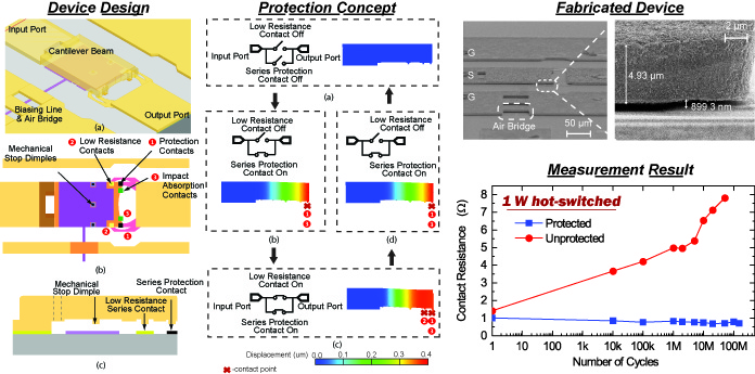
Our group has recently demonstrated an RF-MEMS switch design that can significantly extend the hot-switching life-time of RF-MEMS contact switches. The design concept is shown in the figure above. To prevent the contact degradation during in hot-switching events, a pair of series protection contacts are added in parallel with the "real" contacts. When the switch closes, the protection contacts close first and creates a low-voltage, near cold-switching condition for the "real" contacts. Although protection switches have been proposed in the past, this work combines the protection and "real" contact actuation into a single mechanical structure, and demonstrated unequivocally the significant improvement in hot-switching life-time. For unpackaged devices using Au-Au as the "real" contact material and Pt-Au as the protection contact material, we have demonstrated 150-million actuation cycles at 1-W hot-switching power and 50-million at 2 W. This is much better than anything we have seen!
This design concept can in fact be extended to a few more switch design variations which we are currently investigating. We have also been working on improving the contact materials and packaging for further switch life-time enhancement.
-
Yuhao Liu, Jiansong Liu, Bo Yu, and Xiaoguang Liu, "A Compact Single-Cantilever Multicontact RF-MEMS Switch With Enhanced Reliability," IEEE Microwave and Wireless Components Letters, vol. 28, no. 3, pp. 191-193, Mar, 2018. DOI:10.1109/LMWC.2018.2800523 |

-
Yuhao Liu, Yusha Bey, Xiaoguang Liu, "High-Power High-Isolation RF-MEMS Switches with Enhanced Hot-switching Reliability Using A Shunt Protection Technique," IEEE Transactions on Microwave Theory and Techniques, vol. 65, no. 9, pp. 3188-3199, Apr, 2017. DOI:10.1109/TMTT.2017.2687427 |

-
Yuhao Liu, Yusha Bey, and Xiaoguang Liu, "Extension of the Hot-Switching Reliability of RF-MEMS Switches Using A Series Contact Protection Technique," IEEE Transactions on Microwave Theory and Techniques Applications, vol. 64, no. 10, pp. 3151 - 3162, Oct, 2016. DOI:10.1109/TMTT.2016.2598170 |

-
[Invited]
Yuhao Liu, Hao Wang, Yusha Bey, and Xiaoguang Liu, "A Novel RF-MEMS Shunt Capacitive Switch Design for Dielectric Charging Mitigation," , vol. , no. , pp. , Jul, 2015. DOI:10.1109/IMWS-AMP.2015.7324955 |

-
Yuhao Liu, Yusha Bey, and Xiaoguang Liu, "Single-Actuator Shunt-Series RF-MEMS Switch," , vol. , no. , pp. , Jun, 2014. DOI:10.1109/MWSYM.2014.6848666 |

High-Q Tunable Evanescent-mode Cavity Filters
Tunable filters can significantly reduce the complexity of future software-defined frequency- and bandwidth-agile wireless systems. Achieving wide frequency tuning range and a high unloaded quality factor (Qu) at the same time has long been a challenge for tunable filter design and implementations. Highly loaded evanescent-mode cavity filters offer a great balance between the two requirements.
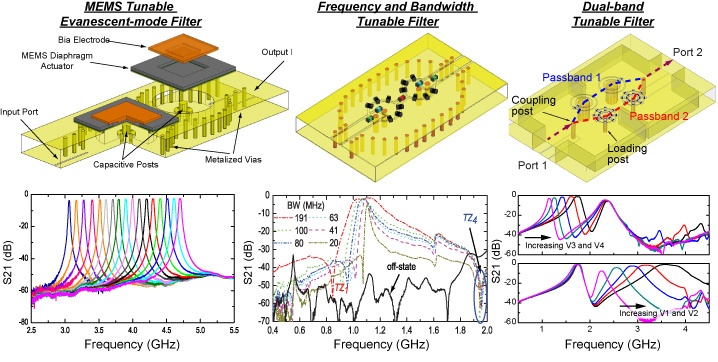
As a graduate student, Dr. Liu pioneered the use of electrostatic micro-electromechanical actuators for the implementation of high-Q tunable evenescent-mode filters. An electronic tunable 2-pole filter was demonstrated for 3-4.7 GHz with 0.7% fractional bandwidth, insertion loss of 3.6-2.4 dB, and extracted Qu of 300-600. Further works demonstrated tunable bandpass and bandstop filters with similarly high Qu and tuning range for frequencies up to 20 GHz.
At UC Davis, we have continued the work exploring various aspects of the design and fabrication of novel tunable filters. We have demonstrated a design strategy for integrating lumped tuning elements with cavity filters. We have also introduced a frequency and bandwidth tunable filter design method based on dispersive coupling structures, showing bandwidth tunability of 0-10%. At the 0% bandwidth state, this coupling structure effectively shuts off the filter and can work as an RF switch without relying on an actual switch. More recently, we have also demonstrated a W-band (75-110 GHz) waveguide tunable filter with recording-breaking tunability and insertion loss.
-
Akash Anand and Xiaoguang Liu, "Reconfigurable Planar Capacitive Coupling in Substrate-Integrated Coaxial-Cavities Filters," IEEE Transactions on Microwave Theory and Techniques, vol. 64, no. 8, pp. 2548-2560, Aug, 2016. DOI:10.1109/TMTT.2016.2580140 |

-
James T. S. Do and Xiaoguang Liu, "A High-Q W Band Tunable Bandpass Filter," , vol. , no. , pp. , May, 2016. DOI:10.1109/MWSYM.2016.7540094 |

-
James Chen, Marvin D. Benge, Akash Anand, Hjali Sigmarsson, and Xiaoguang Liu, "An Evanescent-Mode Tunable Dual-band Filter with Independently-Controlled Center Frequencies," , vol. , no. , pp. , May, 2016. DOI:10.1109/MWSYM.2016.7540404 |

-
Akash Anand and Xiaoguang Liu, "Metallic Air Cavities Integrated with Surface Mount Tuning Components for Tunable Evanescent-Mode Resonators," , vol. , no. , pp. , May, 2016. DOI:10.1109/MWSCAS.2013.6674792 |

-
Akash Anand, and Xiaoguang Liu, "Capacitively Coupled Coaxial-Cavity Bandstop Filters with Tunable Center Frequency and Bandwidth," , vol. , no. , pp. , May, 2015. DOI:10.1109/MWSYM.2015.7167148 |

-
[Best Student Paper]
Akash Anand, and Xiaoguang Liu, "Substrate-Integrated Coaxial-Cavity Filter With Tunable Center Frequency and Reconfigurable Bandwidth," , vol. , no. , pp. , Jun, 2014. DOI:10.1109/WAMICON.2014.6857772 |

-
Akash Anand, Joshua Small, Dimitrios Peroulis, and Xiaoguang Liu, "Theory and Design of Octave Tunable Filters with Lumped Tuning Elements," IEEE Transactions on Microwave Theory and Techniques, vol. 62, no. 12, pp. 4353-4364, Dec, 2013. DOI:10.1109/TMTT.2013.2287674 |

-
Akash Anand, Joshua Small, Muhammad Shoaib Arif, Michael Sinani, Dimitrios Peroulis, and Xiaoguang Liu, "A Novel High-Qu Octave-Tunable Resonator with Lumped Tuning Elements," , vol. , no. , pp. , Jun, 2013. DOI:10.1109/MWSYM.2013.6697760 |

-
Xiaoguang Liu, Linda P. B. Katehi, William J. Chappell, and Dimitrios Peroulis, "High-Q Tunable Microwave Cavity Resonators and Filters using SOI-based RF MEMS Tuners," IEEE/ASME Journal of Microelectromechanical Systems, vol. 19, no. 4, pp. 774-784, Aug, 2010. DOI:10.1109/JMEMS.2010.2055544 |

Systems
In-band Interference Mitigation using RF Correlation
Interference mitigation has arguably become one of the most important issues in modern wireless system design. From a circuit design point of view, bandpass and bandstop filters are conventionally used to attenuate interfering signals outside the bandwidth of the desired signal, but have diminished effectiveness in the presence of in-band interferers. Spread spectrum communication schemes, such as CDMA or frequency hopping, has been used to eliminate in-band interference. However, existing spread spectrum solutions rely on digital signal processing for spreading and de-spreading. In the case of a strong in-band interferer/jammer, the front-end circuit would be desensitized, making it impossible to digitize or process the signal of interest.
In the DARPA Signal Processing at RF (SPAR) program, we are collaborating with Prof. Zhi Ding and Prof. Paul Hurst to work on a new spread spectrum communication architecture for suppressing strong in-band interference. In this architecture, an encoder is placed between the transmitter and the antenna to code the RF waveform with a pseudorandom (PN) sequence. On the receiver end, a correlator and a narrow-band filter are added between the antenna and the low noise amplifier (LNA). When the correlator PN sequence matches that of the transmitter, the original RF waveform can be reconstructed. An in-band interferer, on the other hand, will be spread in spectrum by the correlator. After passing through the narrow-band filter, the power presented at the input of the LNA will be attenuated by a ratio of the spread spectrum divided by the filter bandwidth. This scheme essentially performs CDMA directly at the RF frequency to prevent in-band interference from desensitizing the LNA, thus allowing reliable wireless communication in a hostile electromagnetic environment.
Working together with HRL Laboratories, we are using high-speed Gallium Nitride (GaN) transistors to implement the encoders and the correlators. We are currently in the Phase 3 of the program.
High-speed Chip-to-chip Interconnects at Sub-millimeter-wave and THz Frequencies
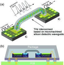
The scaling of semiconductor, especially complementary metal-oxide-semiconductor (CMOS) technologies and massive parallelism of processors have continued to push our computing capabilities to meet today’s data processing demand. However, the rate at which we can move large amounts of data between processors is increasingly becoming a bottleneck for achieving higher computational power. To tackle this challenge, we are investigating high-speed chip-to-chip interconnects solutions using carrier frequencies in the range of 100 GHz - 1 THz. The large amount of bandwidth available at this frequency range makes it an ideal solution for high speed data communication. An enabling technology of this effort is the use of micromachined dielectric waveguide as the interconnect medium, resulting in a significant reduction in link loss. This project in collaboration with Prof. Jane Q. Gu.
-
Bo Yu, Yu Ye, Xuan Ding, Yuhao Liu, Zhiwei Xu, Xiaoguang Liu, and Qun Jane Gu, "Ortho-Mode Sub-THz Interconnect Channel for Planar Chip-to-chip Communications," IEEE Transactions on Microwave Theory and Techniques, vol. 66, no. 4, pp. 1864-1873, Apr, 2018. DOI:10.1109/TMTT.2017.2779496 |

-
Bo Yu, Yu Ye, Xiaoguang Liu, and Qun Jane Gu, "Microstrip line based sub-THz interconnect for high energy-efficiency chip-to-chip communications," , vol. , no. , pp. , Aug, 2016. DOI:10.1109/RFIT.2016.7578183 |

-
Bo Yu, Yu Ye, Xiaoguang Liu, and Qun Jane Gu, "Sub-THz interconnect channel for planar chip-to-chip communication," , vol. , no. , pp. , Jul, 2016. DOI:10.1109/ISEMC.2016.7571770 |

-
Bo Yu, Yuhao Liu, Yu Ye, Xiaoguang Liu, and Qun Jane Gu, "Low-loss and Broadband G-Band Dielectric Interconnect for Chip-to-Chip Communication," IEEE Microwave and Wireless Components Letters, vol. 26, no. 7, pp. 478-480, Jul, 2016. DOI:10.1109/LMWC.2016.2574837 |

-
Bo Yu, Yuhao Liu, Yu Ye, Junyan Ren, Xiaoguang Liu, and Qun Jane Gu, "High Efficiency Micromachined Sub-THz Channels for Low Cost Interconnect for Planar Integrated Circuits," IEEE Transactions on Microwave Theory and Techniques, vol. 64, no. 1, pp. 96-105, Jan, 2016. DOI:10.1109/TMTT.2015.2504443 |

-
Bo Yu, Yuhao Liu, Xing Hu, Xiaoxin Ren, Xiaoguang Liu, and Qun Jane Gu, "Micromachined Sub-THz Interconnect Channels for Planar Silicon Processes," , vol. , no. , pp. , Jun, 2014. DOI:10.1109/MWSYM.2014.6848632 |

-
[Best Conference Paper]
Bo Yu, Yuhao Liu, Xing Hu, Xiaoxin Ren, Xiaoguang Liu, and Qun Jane Gu, "Micromachined Silicon Channels for THz Interconnect," , vol. , no. , pp. , Jun, 2014. DOI:10.1109/WAMICON.2014.6857799 |

Reconfigurable Bandpass Sampling Receivers for Software-Defined Radio Applications
Sponsor: National Science Foundation (NSF), Award #: 1444086
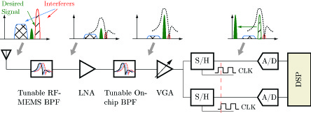
In contrast to a low-pass sampling receiver, the bandpass sampling receiver samples at a much lower frequency with respect to the center frequency of the signal. The analog-to-digital converter (ADC) in the band-pass sampling radio therefore operates at a much lower bandwidth, resulting in a significant reduction in power consumption. The I/Q separation and baseband processing (channel filtering, base-band AGC, etc) can be carried out entirely in the digital domain. This will improve flexibility in terms of adapting to different waveforms and wireless standards. Compared with existing solutions, the tunable bandpass sampling architecture pushes digitization as close to the antenna as possible without having to sacrifice the dynamic range and has the potential to significantly increase the utilization of the ever more crowded radio frequency spectrum.
Wearable Radar Sensor for Long-term Cardiac Arrhythmia Monitoring
Sponsor: National Science Foundation (NSF), Award #: 1549762
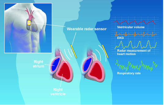
The DART lab has been working with industry partners to apply our expertise in high frequency electronics to medical applications. One example is the use of ultra-low-power radar sensors for the detection of heart health conditions. Contrary to many existing work on radar-based stand-off detection of vital signs, our solution relies on contact-based measurement which significanlty reduces the power consumption, increases the accuracy, and improves noise/clutter rejection.
-
[Accepted]
Heng Zhao, Xiaomeng Gao, Xiaonan Jiang, Hong Hong, and Xiaoguang Liu, "Non-contact Robust Respiration Detection By Using Radar-Depth Camera Sensor Fusion," , vol. , no. , pp. , Jul, 2020. DOI: |

-
[Best Young Professional Paper]
Xiaomeng Gao, Xiaonan Jiang, Songjie Bi, Dennis Matthews, Saul Schaefer, and Xiaoguang Liu, "Measurement of the Complex Human Atrial-Ventricular Motions using Contact-Based Doppler Radar," , vol. , no. , pp. , Apr, 2019. DOI:10.1109/WAMICON.2019.8765441 |

-
Songjie Bi, Xiaonan Jiang, Xiaomeng Gao, Xiaoguang Liu, "Coupling-Cancellation-Antenna for Improving Doppler Radar Motion Measurement Accuracy," , vol. , no. , pp. , Apr, 2019. DOI:10.1109/WAMICON.2019.8765442 |

-
Songjie Bi, Xiaomeng Gao, Victor M. Lubecke, Olga Boric-Lubecke, Dennis Matthews, Xiaoguang “Leo” Liu, "A Multi-Arc Method for Improving Doppler Radar Motion Measurement Accuracy," , vol. , no. , pp. , Jun, 2018. DOI:10.1109/MWSYM.2018.8439687 |

-
Songjie Bi, Juan Zeng, Marzhan Bakbalanova, and Xiaoguang Liu, "Contact-Based Radar Measurement Of Cardiac Motion - A Position And Polarization Study," , vol. , no. , pp. , Jan, 2016. DOI:10.1109/BIOWIRELESS.2016.7445553 |

-
Songjie Bi and Dennis Matthews and Xiaoguang Liu, "An experimental study of 2-D cardiac motion pattern based on contact radar measurement," , vol. , no. , pp. , Apr, 2015. DOI:10.1109/WAMICON.2015.7120390 |
